Cadmium Phosphide (Cd₃P₂)
Cadmium phosphide (Cd₃P₂) is a fascinating compound with a wide range of applications in modern technology. With its formula Cd₃P₂, this semiconductor material is known for its unique properties, including a narrow bandgap of about 0.5 eV. These characteristics make it a go-to choice for high-power electronics, laser diodes, and even emerging fields like biomedical imaging. While its potential is remarkable, handling Cd₃P₂ requires care due to its toxicity, which underscores the importance of proper safety protocols.

What is Cadmium Phosphide?
Cadmium phosphide (Cd₃P₂) is an inorganic compound formed by cadmium and phosphorus. Known for its unique composition and chemical properties, this semiconductor material is used in various applications, from photovoltaic cells to laser diodes. Its narrow bandgap and thermal stability make it a valuable material in electronics, but safe handling is essential due to its toxicity.
Chemical Properties
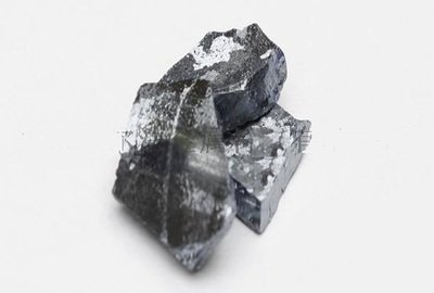
Cadmium phosphide appears as a grey crystalline solid, giving it a distinctive look often used to identify the compound. Here are some of its key chemical properties:
- Molecular Formula: Cd₃P₂
- Molecular Weight: Approximately 399.18 g/mol
- Melting Point: Around 700°C
- Density: About 5.96 g/cm³
These properties make cadmium phosphide suitable for high-temperature applications, especially in environments where thermal resilience is critical. For further details on its chemical properties, check the Cadmium Phosphide profile at PubChem.
Synthesis of Cadmium Phosphide
Synthesising cadmium phosphide involves several methods and techniques tailored to ensure high purity and precise composition. Here’s an overview of the common methods:
- Direct Reaction:
- This process involves reacting cadmium metal directly with phosphorus.
- The reaction requires controlled conditions to prevent side reactions.
- It’s one of the simplest and most commonly used methods for producing Cd₃P₂.
- Thermolysis:
- Another approach is heating cadmium-containing compounds in the presence of a phosphorus source.
- This high-temperature process decomposes organic precursors, leaving behind cadmium phosphide.
- Chemical Vapour Deposition (CVD):
- Gaseous cadmium and phosphorus react in a vacuum chamber to form a thin layer of Cd₃P₂.
- This method is preferred for creating films used in semiconductor applications.
Each method has its advantages, often chosen based on the application or required scale of production. For detailed insights into modern synthesis techniques, explore this preparation method for cadmium phosphide materials.
Understanding both its chemical properties and synthesis methods highlights the adaptability of cadmium phosphide in advanced systems, while reinforcing the need for responsible handling due to its potential hazards.
Applications of Cadmium Phosphide
Cadmium phosphide (Cd₃P₂) is more than just a chemical compound—it’s a vital player in modern technology. Its unique properties as a semiconductor have made it indispensable in electronics, energy, and emerging technologies. Below, we explore its most significant applications, from tried-and-true uses to exciting innovations shaping the future.
Use in Electronics
Cadmium phosphide finds widespread use in electronics, especially in high-power, high-frequency devices. Thanks to its electrical properties, it excels in areas where efficiency and durability matter. For example:
- Optoelectronic Devices: Cadmium phosphide is a key material in laser diodes and photodetectors, enabling efficient light generation and detection.
- High-frequency Electronics: Devices such as transistors and amplifiers use this compound for its ability to perform under intense operating conditions.
These features make Cd₃P₂ essential across industries, from telecommunications to defence systems. For detailed technical specs, refer to the American Elements resource on cadmium phosphide.
Semiconductor Properties
As a semiconductor, cadmium phosphide boasts a narrow direct bandgap, which makes it ideal for energy conversion and photonic applications. Its properties include:
- Suitability for Solar Cells: Cd₃P₂ effectively absorbs sunlight, making it a promising candidate for photovoltaic cells. This capability positions it as part of the ongoing search for high-efficiency solar technologies.
- Applications in Laser Diodes: Its optical characteristics enable it to emit coherent laser light, often used in high-precision equipment and communication systems.
- Quantum Technology: Early research suggests cadmium phosphide-based nanostructures, like quantum dots, could become standard in high-performance displays and imaging.
For a more in-depth look, check out this early study on the semiconducting properties of cadmium-based materials.
Emerging Applications
The future of cadmium phosphide is bright, especially as research pushes the boundaries of its capabilities. Some of the most exciting uses on the horizon include:
- Near-Infrared Emission: Cd₃P₂ is being explored for its ability to emit near-infrared light, which is crucial for applications in night vision and medical imaging.
- Innovative Quantum Dot Technologies: With the demand for cutting-edge displays and lighting increasing, cadmium phosphide-enabled quantum dots may soon offer unmatched performance and colour accuracy.
- Infrared Converters: Studies are investigating Cd₃P₂ for infrared sensor systems, which play a role in everything from climate monitoring to advanced security equipment. Learn more about these developments in this research publication on infrared converters.
As these breakthroughs progress, cadmium phosphide is poised to remain at the forefront of innovation. Stay updated on related technologies by exploring quantum dot advancements in modern applications.


