NDIUM PHOSPHIDE Chemical Properties
| Melting point | 1070°C |
| density | 4,787 g/cm3 |
| solubility | slightly soluble in acid solutions |
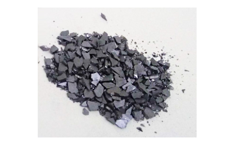
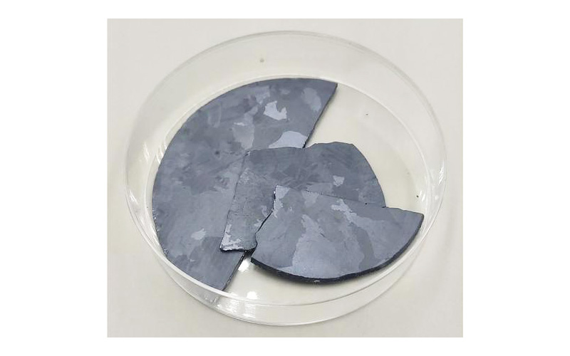
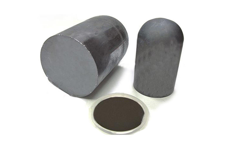
| form | pieces |
| color | Black |
| Water Solubility | Insoluble in water. |
| Crystal Structure | Cubic, Sphalerite Structure – Space Group F(-4)3m |
| Boiling Point | N/A |
| Exposure limits | ACGIH: TWA 0.1 mg/m3 NIOSH: TWA 0.1 mg/m3 |
Safety Information
| RIDADR | 3288 |
| WGK Germany | 3 |
| RTECS | NL1800000 |
| TSCA | Yes |
| Hazardous Substances Data | 22398-80-7(Hazardous Substances Data) |
| Toxicity | mouse,LD,intraperitoneal,> 5gm/kg (5000mg/kg),ENDOCRINE: CHANGES IN SPLEEN WEIGHTLUNGS, THORAX, OR RESPIRATION: CHANGES IN LUNG WEIGHTBLOOD: “CHANGES IN SERUM COMPOSITION (E.G., TP, BILIRUBIN, CHOLESTEROL)”,Journal of Occupational Health. Vol. 38, Pg. 6, 1996. |
INDIUM PHOSPHIDE Usage And Synthesis
| Chemical Properties | black crystal(s); 6mm pieces and smaller with 99.999% purity; semiconductor; band gap, eV, 1.42 (0K) and 1.35 (300K); mobility (300K), cm2/(V·s), 4600 electrons and 150 holes; dielectric constant 12.4; effective mass 0.077 electrons and 0.64 holes [KIR82] [CER91] [STR93] |
| Uses | InP is used in high-power and high-frequency electronics because of its superior electron velocity. It also has a direct bandgap, making it useful for optoelectronics devices like laser diodes. It is also used as a substrate for epitaxial indium gallium arsenide based opto-electronic devices.Used as semiconductor material for optical fiber communication technology, it requires a light source and receiver in the range of 1.1 to 1.6 μm. Growing In-GaAsP double heterojunction lasers on InP substrates can meet both lattice matching and wavelength range requirements. |
| Uses | In electronics for research on semiconductors. |
| Flammability and Explosibility | Not classified |
| Production method | The main method is to prepare indium phosphide single crystals using a high-pressure single crystal furnace, and to reduce the dislocation density of the crystal by doping with isoelectronic impurities. For vapor phase epitaxy, the disproportionation method of the In-ChemicalbookPCl3-H2 system is mostly used. In this process, the indium phosphide layer is grown by the reaction between indium (99.9999%) and phosphorus trichloride (99.999%). |
| Gas phase epitaxy places the quartz reaction tube in a double-temperature zone electric furnace, and the purified high-purity hydrogen is metered in. The hydrogen is also used to dilute the phosphorus trichloride. At this time, the bubbler is kept at 0°C, and the linear velocity of the hydrogen passing through the reaction tube is 14cm/min. Epitaxial growth is carried out in two stages. | |
| In the first stage, the quartz boat containing indium is placed in the source zone of the electric furnace, hydrogen is introduced and heated to 700-850°C, and then phosphorus trichloride is introduced with hydrogen, which is reduced to phosphorus vapor and hydrogen chloride above the indium source. Cadmium hydrogen reacts with indium to generate indium monochloride vapor that migrates in the tube. Phosphorus dissolves in indium until saturated. | |
| In the second stage, the indium source is kept in its original position without heating. After the single crystal substrate is placed in the second heating zone of the electric furnace, it is heated to 600-750°C in a hydrogen atmosphere. First, phosphorus trichloride is introduced into the tube with hydrogen to perform vapor phase etching on the substrate and clean the substrate surface. Then, hydrogen is directly introduced into the reaction tube, and the source is heated to its supersaturation temperature (this temperature is 100°C higher than the temperature of the substrate crystal during operation). Phosphorus trichloride is then introduced through hydrogen bubbling, and the phosphorus vapor reacts with the indium monochloride generated in the source area to deposit and grow an indium phosphide layer on the substrate. When the epitaxial growth is completed, pure hydrogen is introduced into the system, the two temperature zones are cooled to room temperature, and the product is taken out to obtain the finished indium phosphide product. |
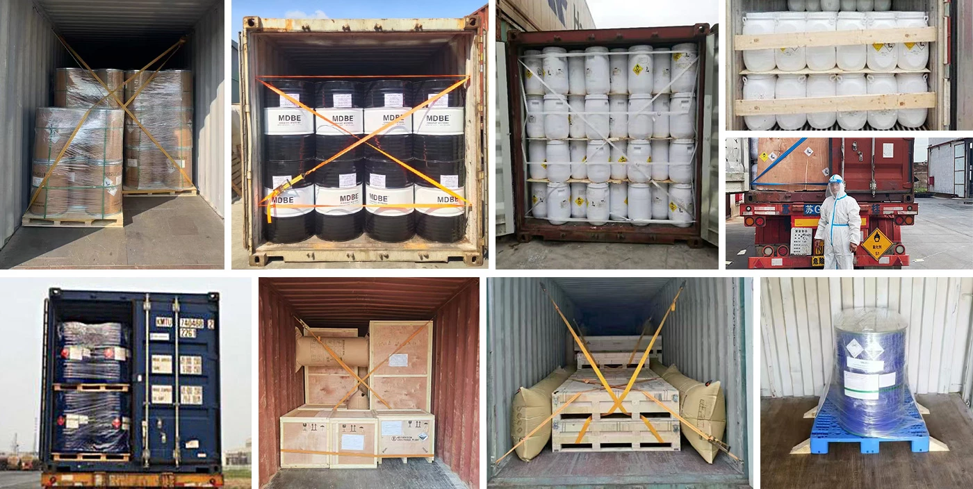
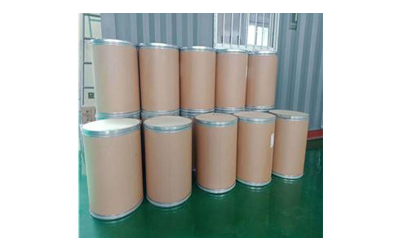
Our company specializes in hazardous chemicals, flammable and explosive chemicals, toxic chemicals (legal export), ultra-pure and high-purity reagents. Welcome to contact us.
Packing and shipping
